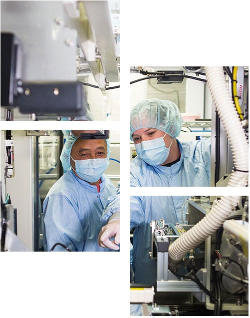
pSemi has a 30-year history of leading semiconductor technology development. From the invention of RF SOI to our innovation in the RF front end, our team continuously transforms what “can’t be done” into an industry first. After decades of advancing SOI for RF applications, we now readily apply other semiconductor technologies to further optimize our product offerings. We focus both on the process and the overall solution. We continue to develop custom processes—as in our proprietary UltraCMOS® technology platform—but we also leverage off-the-shelf technologies. Our team evaluates each solution and uses the best combination of state-of-the-art semiconductor technologies to meet the market’s requirements.
Our UltraCMOS® technology—a patented, advanced form of silicon-on-insulator (SOI)—enables pSemi to offer a market-leading combination of large- and small-signal performance. With its outstanding RF and microwave properties, SOI provides an ideal substrate for integration. When paired with high-volume CMOS—the most widely-used semiconductor technology—the result is a reliable, repeatable technology platform that offers superior performance compared to other mixed-signal processes.

30 Years of SOI Innovation
Our team pioneered the use of SOI for RF applications using sapphire substrates because of their ultra-pure and near-perfect insulator qualities. Today, we maintain a leadership advantage in SOI process technology. Our process development is custom, our process selection is flexible and controlled, and our cycle time and quality are proven.

Superior RF Performance
Our UltraCMOS technology platforms lead the industry in RonCoff performance. RonCoff is a key performance metric of an RF switch, which is controlled to turn “on” (a resistor) or “off” (a capacitor). A low resistance (Ron) reduces insertion loss, and a low capacitance (Coff) increases isolation. In RF switching, performance is optimal when both metrics are as low as possible.
Continuous Optimization
With each generation of the UltraCMOS technology platform, we further optimize the technology for the latest market requirements. Our UltraCMOS 13 platform is manufactured in high-volume 300 mm foundries and targets 5G-NR sub-6 GHz applications. It provides our low-noise amplifiers (LNAs), power amplifiers (PAs) and switches with enhanced performance, including ultra-low leakage FETs for PAs, lower NFmin for LNAs, high-power handling for switches, and optimized analog and digital support.